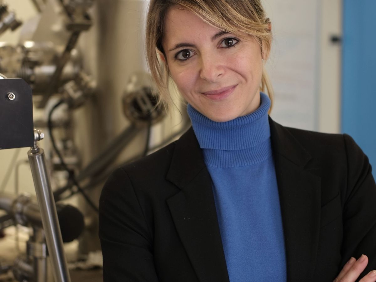
Interview with Camilla Coletti, Coordinator of IIT’s Center for Nanotechnology Innovation (CNI@NEST)
The church of San Silvestro in Pisa, which has not been used for worship for many years, was built before 1118 and entrusted to the Benedictine monks of Montecassino. Later, the church and convent were used by nuns in the Dominican order. The convent then became the first premises for the Scuola Normale Superiore founded by Napoleon in 1810. It is here, in this location rich in history and culture, that the IIT Center for Nanotechnology Innovation, directed by Camilla Coletti, is sited.
Camilla, could you give us some historical background on the Center?
The Center for Nanotechnology Innovation (CNI) was founded in 2009, with two directions. The first focuses on low-dimensional materials such as graphene, a substance that was discovered only in 2004 and about which little was known in Italy at the time. The second area is nanomedicine, with nanotheranostics for the diagnosis and treatment of cancer through an AIRC (Associazione italiana per la Ricerca sul Cancro, Italian cancer research association) project, and another branch studying nanoproteins and biostructures. About 40 people work at this centre and we have state-of-the-art technological equipment. The quality of the staff and the machines are a combination that enables us to approach the future with great confidence.
What is the profile of your researchers?
We are a multicultural group, and this is demonstrated by my researchers’ countries of origin. Here, Finns, Lithuanians, Russians, Poles, Ethiopians, Filipinos and Indians operate together. Algerian, Ukrainian, Korean, Iraqi, German, American and Turkish researchers have worked with us in the recent past. The proportion of women in the staff at our laboratories reaches 45%. A significant percentage.
How long have you been working at IIT?
I joined the Foundation in 2011 as a senior postdoc. I came from the Max Planck Institute after spending some time working on my studies in various locations around the world, from Zurich for my dissertation, to Florida for my PhD and then to Stuttgart. Returning to Italy was not easy, for the reasons that are all too familiar. Looking back to my attempt to return to the world of research in Italy, I remember the detail that put me into contact with IIT. My time abroad had accustomed me to using English, so I was looking for new opportunities offered in this language. And I couldn’t find anything. The only job post in English was one at IIT. I applied, had an interview with Fabio Beltram, who at that time was the Center’s coordinator, and about a year after those interviews I began my work at CNI. During the first year, we developed the instrumentation that would be used to synthesise highly crystalline graphene, a very clean, high-performance material, and later Vittorio Pellegrini developed studies on inks at IIT. My career path has developed from that period right through to the present day: I became a researcher, then I moved into a tenure track position and, since last year, I have become ‘stabilised’, as we call it in our internal language, taking over the Center’s coordination.
From Max Planck to IIT. How did you experience this transition?
I came from an organisation that is one of the best options in the world as far as research is concerned. I was working in the department of Nobel Prize winner Klaus von Klitzing and I had the opportunity to acquire crucial knowledge on the study of graphene, as well as coming into contact with leading figures in the international scientific community. However, I missed my own country, and the scientific background that I had acquired enabled me to leave Stuttgart. So I ended up amidst the arches of the cloisters at the Church of San Silvestro in Pisa, where IIT is located, and I found excellent resources in terms of technological equipment. When compared to the Max Planck Institute, IIT has allowed me to grow professionally and to take on direct responsibilities. So I have experienced two different phases in my professional career, with no regrets about having left the former.
However, your important commitment at IIT coincided with an event of immeasurable human importance: becoming a mother. How did you manage to reconcile work and family?
It was a difficult time because I had to deal with the bureaucratic obstacles that precluded me from operational spaces during my pregnancy. I therefore tried to be proactive during that period, looking for talented collaborators who could help me. So in 2012 I hired Vaidas, a Lithuanian, who was then a postdoc, and is now still part of the group as a contract technologist, who started working with me a month before my first daughter was born. At that time, I was denied access to the laboratory for security reasons and had to seek several medical opinions in order to be able to continue my work. If I had not been so determined at that time, probably I would not be here today.
Your story gives us the chance to touch on a very important issue, the difficulties women still have to deal with in the world of work. How do you feel about this today?
Things are definitely improving, albeit in small steps. There is still a big difference between the situation in this area in our country and, for example, that in northern Europe, where parental leave is identical for both women and men. IIT has made positive efforts to try to change this state of affairs by setting up an office for inclusion and diversity in order to identify the needs of minorities, and certainly in our sphere, women are a minority group. In addition to that, decisions have to be adopted by the country’s institutions, especially to prevent women from abandoning their jobs in the face of the difficulties that they encounter.
Is there a characteristic that you would like to underline when describing the typical profile of a female researcher?
Determination. I can give you an example to illustrate this statement. In the course of my career I have always seen that women who start a university course go on to complete it. For example, in my degree course there were two hundred of us in the first year, a number that had gone down to thirty in the last year. There were six women at the start of the degree course, and all six graduated. There weren’t many women, but they were undoubtedly highly motivated and, as I said, very determined. When it comes to the working environment, women are often an element of balance, making it easier to handle relationships in a relaxed way.
Let’s return to graphene. Today people talk about it in terms of a familiar and much-used material, and its novelty effect seems to have worn off. But research into graphene continues.
The discovery and study of graphene’s properties have revealed this material’s incredible characteristics. It is made up of carbon and often a single atom, and over the course of a short period of time it has proved to be a veritable playground for physicists. In this material, the charge carriers, electrons and holes, move at ballistic speeds, comparable to that of light. After this exciting period, promising applications have been identified in various fields such as electronics, sensors, energy storage and generation. Scientists have successively focused on creating large-scale, cost-effective synthesis processes for the material. Over the years, two main synthesis techniques have been developed: the production of inks by means of graphite exfoliation processes, and the synthesis of highly crystalline graphene in high-temperature kilns. In recent years, graphene inks have been used in a large number of low-tech applications: there are textile and plastic products on the market in which graphene offers an added value by increasing the strength, flexibility, and conductivity of the initial materials to which it is added. In our laboratories at CNI, we specialise in the technique of manufacturing highly crystalline graphene in kilns. This area of graphene research is progressing more slowly than that dedicated to inks. In this case, quality control – graphene must comply with very stringent requirements – is very thorough, and the high-tech applications of graphene take longer because they are more sophisticated.
Over the last few years, highly crystalline graphene has attracted a lot of interest worldwide, with an outlook for high-performance, low-energy applications in various fields. For example, as part of the European Graphene Flagship project, we have demonstrated, together with major multinational companies and other research centres, graphene’s potential in photonic applications, more specifically in the field of telecommunications. We are all very aware – as the pandemic has unfortunately shown us – of how important it is to be connected to the internet and to be able to communicate using mobile devices. Graphene has a series of properties that make it possible to make devices for transmitting and receiving data that are small, very fast and with a low energy consumption. This is a very important area of application for graphene, which is being closely observed, together with us, by leading players in the telecommunications system, attracting considerable funding from the European Community. For example, very recently we have received funding for an important European project, of the Research and Innovation Actions (RIA) type, on these themes.
Lastly, basic research on graphene is constantly developing, notwithstanding the passage of time. Graphene has made it possible to open up a new and promising field of study, that of twistronics. This involves placing two sheets of graphene on top of each other at a controlled angle so that the electronic properties of the resulting double layer, which can be either insulating or conductive, can be radically altered. If you manage to achieve what is known as the ‘magic angle’, you can make a superconductive material with very interesting qualities. More in general, by stacking two-dimensional materials, you can obtain highly innovative substances whose properties differ completely from those of the individual constituent layers. Research into two-dimensional materials is a constant source of new discoveries. For example, we have recently observed that gold, the quintessential metal, becomes a semiconductor when limited to two-dimensional form.
This is a direction of basic research that encourages new science, new discoveries and, we hope, important funding.